Details
STM32 development board, STM32F407IGT6, USB HS/FS, Ethernet, NandFlash, JTAG/SWD, LCD, USB TO UART
Overview
EVK407I is an STM32 development board which consists of a mother board and a MCU core board XCore407I.
What's on the mother board

- MCU core board connector
- MCU pins expander
- JTAG/SWD interface, for debugging/programming
- LCD interface, for connecting touch screen LCD
- USB connector, USB TO UART
- 5V DC jack
- PL2303TA, onboard USB TO UART controller
- PL2303 jumper
- User LED jumper
- Joystick jumper
- 12M crystal, PL2303 clock
- User LEDs, convenient for indicating I/O status and/or program running state
- UART LEDs, UART TX/RX indicator
- Joystick
For jumpers 8-10:
- short the jumper to connect to I/Os used in example code
- open the jumper to connect to other custom pins via jumper wires
What's on the MCU core board

- STM32F407IGT6:the high performance STM32 MCU which features:
- Core: Cortex-M4 32-bit RISC
- Feature: a full set of single-cycle DSP instructions
- Operating Frequency: 168MHz, 210 DMIPS/1.25 DMIPS/MHz
- Operating Voltage: 1.8V-3.6V
- Package: LQFP176
- Memories: 1024kB Flash, 192+4kB SRAM
- MCU communication Interfaces:
- 3 x SPI, 4 x USART, 2 x UART, 2 x I2S, 3 x I2C
- 1 x FSMC, 1 x SDIO, 2 x CAN
- 1 x USB 2.0 high-speed/full-speed device/host/OTG controller with dedicated DMA, ULPI and on-chip full-speed PHY
- 1 x 10/100 Ethernet MAC
- 1 x 8 to 14-bit parallel camera interface
- AD & DA converters: 3 x AD (12-bit, 1μs, shares 24 channels); 2 x DA (12-bit)
- Debugging/Programming: supports JTAG/SWD (serial wire debug) interfaces, supports IAP
- MIC2075-2, onboard USB FS power management device
- AMS1117-3.3, 3.3V voltage regulator
- K9F1G08U0E, 1G Bit NandFlash
- DP83848, Ethernet PHY
- MIC2075-1, onboard USB HS power management device
- USB3300, USB HS PHY
- Power supply switch, powered from 5Vin or USB connection
- Boot mode switch, for configuring BOOT0 pin
- Power indicator
- USB FS LED
- USB HS LED
- Reset button
- 8M crystal, MCU clock, enables the MCU run at higher speed by frequency multiplication
- 24M crystal, USB3300 clock
- 50M crystal, DP83848 clock
- 32.768K crystal, for internal RTC with calibration
- Ethernet connector
- USB FS mini connector
- USB HS mini connector
- USB HS type A connector
- MCU pins expander, VCC, GND and all the idle I/O ports are accessible on expansion connectors for further expansion
- USB OTG/HOST jumper
- VREF/VBAT jumper
- Ethernet I/O selection solder joint
- USB HS I/O selection solder joint
- PDR selection solder joint: 1.8-3.6V, -40~105℃ OR 1.7-3.6V, 0~70℃
Photos
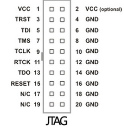
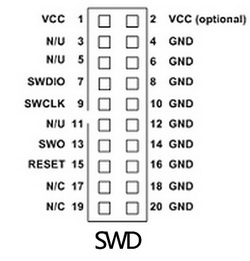
JTAG/SWD interfaces
The figure 1, and 2 show the header pinouts of JTAG/SWD interface
Figure 1. JTAG Header Pinout


Figure 2. SWD Header Pinout


Development Resources
- Related software (KEIL etc.)
- Examples in C
- Schematic (PDF)
- Development documentations


